Digital computers perform a varity of information processing tasks. Among the basic tasks encountered are the various arithmatic operartions. The moest basic arithmatic operation is the additon of two binary digits. This simple addition consist of 4 possible operations, they are 0+0=0, 0+1=1, 1+0=1, 1+1=1 and 1+1=10.
The first three operations produce a sum whose length is one digit, but when both augund and addend bits are equal to 1, the binary sum consists of two digits. The higher significant bit of this result is called a carry. When the augend and addend number contain more significant digits, the carry obtained from from the addition of two bits is added to the next higher order pair of significant bits. A combinational circuit that performs the addition of two bits is called a half adder. Again the combinational circuit that performs addition of three bits (Two significant bits and a previos carry) is called Full adder.
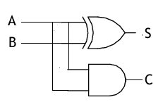
A half adder is a combinational cuircuit with two binary inputs (augend and addend bits) and two binary outputs (sum and carry bits). It adds two inputs (A and B) and produces the sum (S) and the carry (C) bits. It is an arithmatic circuit used to perform the arithmatic operaton of addition of two single bit words.
| Inputs | Outputs | ||
|---|---|---|---|
| A | B | C | S |
| 0 | 0 | 0 | 0 |
| 0 | 1 | 0 | 1 |
| 1 | 0 | 0 | 1 |
| 1 | 1 | 1 | 0 |
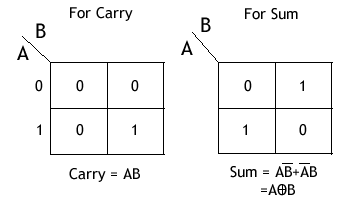
According to rules of binary addition, the sum bit (S) and the carry bit (c) are as follws:
The sum bit (S) is the XOR of A and B. So we have S=AB'+A'B=A⊕B
Again the cary bit (C) is the AND of A and B. So C=AB.
In Multidigit addition we have to add two bits alongwith the carry of the previous digit addition. Effectively such addition requires addition of three bits. This is not possible with half adder.
We used the following components for this experiment-
After Starting the experiment first click on the Components button to get component list. Now you can Drag and Drop any component in the circuit designing area. To make connection between components, just click on the Blue bubble of any components and Drag it to another Blue bubble of the same or any other components. To delete connection or to remove any component use Double click on that component or connection.
Connect the Vcc and Ground pins of the ICs with the power supply. Now connect the input pins of the ICs with the Input Switches. Connect the output pins with output LEDs. Only pins with Blue bubbles can be used.
Green LEDs are used for indicating logic 0 and Red LEDs are used for logic 1.
After connecting all the required components, click on the Start button.