An adder is digital circuit that perform addition of numbers. In modern computer adder resides in the arithmetic logic unit (ALU). There are two types of Adder:
Half Adders are the most basic of the adders. The half adder accepts two binary digits on its inputs and produce two binary digits outputs, a sum bit and a carry bit.
| Inputs | Outputs | ||
|---|---|---|---|
| A | B | C | S |
| 0 | 0 | 0 | 0 |
| 0 | 1 | 0 | 1 |
| 1 | 0 | 0 | 1 |
| 1 | 1 | 1 | 0 |
The full adder accepts two inputs bits and an input carry and generates a sum output and an output carry. The first two inputs are A and B and the third input is an input carry designated as Cin. When a full adder logic is designed we will be able to string four of them together to create a 4 bit adder and cascade the carry bit from one adder to the next.
The output carry is designated as Cout and the normal output is designated as S.
| Inputs | Outputs | |||
|---|---|---|---|---|
| A | B | Cin | S | Cout |
| 0 | 0 | 0 | 0 | 0 |
| 0 | 0 | 1 | 1 | 0 |
| 0 | 1 | 0 | 1 | 0 |
| 0 | 1 | 1 | 0 | 1 |
| 1 | 0 | 0 | 1 | 0 |
| 1 | 0 | 1 | 0 | 1 |
| 1 | 1 | 0 | 0 | 1 |
| 1 | 1 | 1 | 1 | 1 |
In electronics, a multiplexer (or MUX) is a device that selects one of several analog or digital input signals and forwards the selected input into a single line. A multiplexer of 2n inputs has n select lines, which are used to select which input line to send to the output. Multiplexers are mainly used to increase the amount of data that can be sent over the network within a certain amount of time and bandwidth. A multiplexer is also called a data selector.
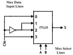
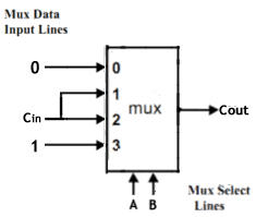
Multiplexer is also called a data selector,whose single output can be connected to anyone of N different inputs. A 4 to 1 line multiplexer has 4 inputs and 1 output line.In our experiment,we use IC 74153(Multiplexer) and IC 7404(NOT gate) for implementing the full adder.
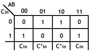
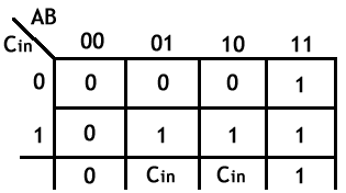
In our experiment, A,B,Cin are the inputs and S,Cout are the outputs.Now implementation function for sum and carry out are as followes.
S(A,B,Cin)= ∑(1,2,4,7)
Cout(A,B,Cin)= ∑(3,5,6,7)
For sum out:
For carry out:
Logic digram for Sum out
Logic digram for Carry out
We used the following components for this experiment-
After Starting the experiment first click on the Components button to get component list. Now you can Drag and Drop any component in the circuit designing area. To make connection between components,just click on the Blue bubble of any components and Drag it to another Blue bubble of the same or any other components. To delete connection or to remove any component use Double click on that component or connection.
Connect the Vcc and Ground pins of the ICs with the power supply. Now connect the input pins of the ICs with the Input Switches. Connect the output pins with output LEDs. Only pins with Blue bubbles can be used.
Green LEDs are used for indicating logic 0 and Red LEDs are used for logic 1.
After connecting all the required components, click on the Start button.
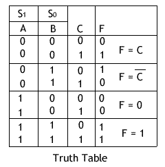
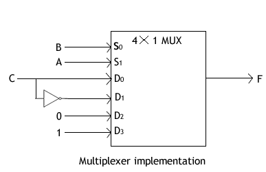
Q: Use 4 to 1 MUX implement the logic function:
F(A,B,C) = ∑(1,2,4,7)
ANS: