Digital computers perform a varity of information processing tasks. Among the basic tasks encountered are the various arithmatic operartions. The moest basic arithmatic operation is the additon of two binary digits. This simple addition consist of 4 possible operations, they are 0+0=0, 0+1=1, 1+0=1, 1+1=1 and 1+1=10.
The first three operations produce a sum whose length is one digit, but when both augund and addend bits are equal to 1, the binary sum consists of two digits. The higher significant bit of this result is called a carry. When the augend and addend number contain more significant digits, the carry obtained from from the addition of two bits is added to the next higher order pair of significant bits. A combinational circuit that performs the addition of two bits is called a half adder. Again the combinational circuit that performs addition of three bits (Two significant bits and a previos carry) is called Full adder.
A full adder is a combinational circuit that performs that adds two bits and a carry and outputs a sum bit and a crry bit. When we want to add two binary numbers ,each having two or more bits,the LSBs can be added by using a half adder. The carry resulted from the addition of the LSBs is carried over to the next significant column and added to the two bits in that column. So, in the second and higher columns, the two data bits of that column and the carry bit generated from the addition in the previous column need to be added.
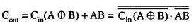
The full adder adds the bits A and B and the carry from the previous column called the carry in (Cin) and the outputs the sum bit (S) and the carry bit called the carry out (Cout). The variable S gives the value of the least significant bit of the sum. The variable Cout gives the outout carry.
| Inputs | Outputs | |||
|---|---|---|---|---|
| A | B | Cin | S | Cout |
| 0 | 0 | 0 | 0 | 0 |
| 0 | 0 | 1 | 1 | 0 |
| 0 | 1 | 0 | 1 | 0 |
| 0 | 1 | 1 | 0 | 1 |
| 1 | 0 | 0 | 1 | 0 |
| 1 | 0 | 1 | 0 | 1 |
| 1 | 1 | 0 | 0 | 1 |
| 1 | 1 | 1 | 1 | 1 |
The above truth table shows all possible combination of 1's and 0's that these varible may have. The 1's and 0's for output variables are detrmined from the arithmatic sum of the input bits. When all input bits are 0, the output is 0. The S output is equal to one when only one input is equal to 1 or three inputs are equal to 1.The c output has carry of 1 if two or three inputs are equal to 1.
From the truth table, we make the following K-map.
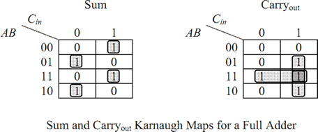
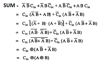
From the above K-map,the logical simplified expression for carry out and sum are

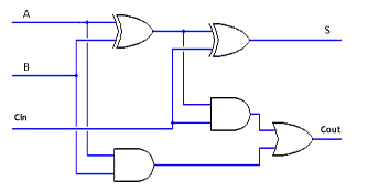
The following Logic diagram shows how 1bit Full Adder is implimented using AND,OR and XOR gates.
We used the following components for this experiment-
After Starting the experiment first click on the Components button to get component list. Now you can Drag and Drop any component in the circuit designing area. To make connection between components,just click on the Blue bubble of any components and Drag it to another Blue bubble of the same or any other components. To delete connection or to remove any component use Double click on that component or connection.
Connect the Vcc and Ground pins of the ICs with the power supply. Now connect the input pins of the ICs with the Input Switches. Connect the output pins with output LEDs. Only pins with Blue bubbles can be used.
Green LEDs are used for indicating logic 0 and Red LEDs are used for logic 1.
After connecting all the required components, click on the Start button.
Implement full adder using NAND gates.
Ans: Implementation of full adder using NAND gates is as follows.
The logic digram is geven bellow.
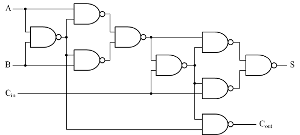
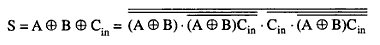
As we seen in the above logic digram, here we use nine nand logic gates. The sum output is
The carry output is